Silicon wafer manufacturing process pdf
Silicon production processes. To meet the needs of a solar-dominated future, high-purity silicon companies are exploring process improvements mainly for two chemical vapor deposition (CVD) approaches — an established production approach known as the Siemens process, and a manufacturing scheme based on fluidized bed (FB) reactors.
Contamination is defined as a foreign material at the surface of the silicon wafer or within the bulk of the silicon wafer. The contamination can be particles or ionic contamination,
The Technology Foundry for a Digitally-Connected World. SkyWater is a different kind of foundry. We provide semiconductor manufacturing solutions for companies looking to design and scale new technologies in a US-owned, risk-reduced manufacturing environment.
Intel Corporation
THE MANUFACTURING PROCESS n Overview of manufacturing process n Design rules n IC packaging Future Trends in Integrated Circuit Technology 2.1 Introduction 2.2 Manufacturing CMOS Integrated Circuits 2.2.1 The Silicon Wafer 2.2.2 Photolithography 2.2.3 Some Recurring Process Steps 2.2.4 Simplified CMOS Process Flow 2.3 Design Rules — The Contract between Designer and Process …
During the slicing process, the wafer is cut from the produced silicon ingot. The The wafer is typically cut to a thickness of 1- 1.5 mm by an extremely fine slicing wire.
Download PDF Info Publication number US6284658B1 The present invention relates to a manufacturing process for a semiconductor wafer and more particularly, to a manufacturing process for a silicon single crystal wafer. 2. Description of the Prior Art. Conventionally, a manufacturing process for a semiconductor wafer, as shown in FIG. 5, has in general comprised: a slicing step E …
manufacturing process pdf The basic processing steps used in fabricating integrated devices will be examined in this lecture, then the use of these process steps in.Recent gate material in nanoscale processes is back to metal.
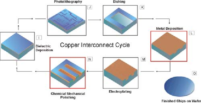
Robotics (wafer handling) is omnipresent in the fab. The semiconductor manufacturing process flow, when highly simplified, can be divided into two primary cycles of
The popular Czochralski method uses a small piece of solid silicon (seed) which is placed in a bath of molten silicon, or polycrystalline silicon, and then slowly pulled in rotation as the liquid grows into a cylindrical ingot. This is why the finished wafers are all round discs.
Silicon Wafer Manufacturing Process What others are saying “A new germanium-tin laser could be used to speed data transfers within CPUs and integrate more easily with existing manufacturing .”
Manufacturing Process of Silicon WaferauthorSTREAM
Polysilicon Production Chemical Engineering Page 1
AWWA/AMTA© 1 NOVEL ULTRAFILTRATION OPERATING PROCESS FOR SILICON WAFER PRODUCTION WASTEWATER REUSE Ben Freeman Hydranautics – A Nitto Group Company
CMOS Process Flow • Overview of Areas in a Wafer Fab – Diffusion – Photolithography – Etch – Ion Implant – Thin Films – Polish • CMOS Manufacturing Steps • Parametric Testing • 6~8 weeks involve 350-step. Semiconductor Manufacturing Technology 5/41 by Michael Quirk and JulianSerda Model of Typical Wafer Flow in a Sub-Micron CMOS IC Fab Test/Sort Implant Diffusion Etch
wafer silicon manufacturing process The primary processing steps for the production of silicon solar cells from quartz are as. Metallurgical route to solar-grade silicon, wafer manufacturing, and, lastly, silicon solar cell. Oltaicsuntil2014.pdf. Zhang and.The supply of bulk silicon has given way to the manufacturing of advanced materials. Without significantly improving and controlling
Grinding is an important process for manufacturing of silicon wafers. The demand for silicon The demand for silicon wafers with better quality and lower price presents tremendous challenges for …
For more than 40 years, Sil’tronix Silicon Technologies aims to manufacture monocrystalline silicon wafer. We manage the whole manufacturing process by the achievement of the entirely production within our own factory.
A silicon wafer is a thin slice of crystalline silicon used in electronics for the fabrication of integrated circuits and in photovoltaics for conventional, wafer-based solar cells.
Lecture 21: Silicon wafer manufacturing Contents 1 Introduction 1 2 Poly Si manufacture 2 3 Single crystal Si manufacture 5 3.1 Czochralski crystal growth technique
• Silicon compatible process; fabless, using high-volume 150mm CMOS foundry for manufacturing; low-cost. 150mm SiC Wafers – Game Changer 3 Power Logic SiC Silicon 6”: 225% the area of 4” • SiC power devices can be manufactured in 150mm silicon fabs. • This is a technology that can be manufactured in US cost effectively. • Monolith was formed with this vision. • XFab, Texas is
cut silicon wafer and chip packaging are not designed to cut hard material. As a result, manufacturers are having extreme difficulties bringing the process to profitable, high-volume manufacturing. Silicon carbide (SiC) is the third hardest compound material on earth with material hardness of 9.5 on the Mohs scale. The wafers are extremely difficult to cut because they are almost as hard as

IC Manufacturing Process Group 6. Purification • Silicon is found in quartzite • Second most abundant element behind oxygen • Other elements must be removed • Quartzite heated to 2000⁰C then purified again through a chemical process • Silicon is now in rod form and sawed into wafers. Wafer Preparation • Wafer is polished to be almost mirror like • Final chemical process removes
A patented closed-loop manufacturing process results in minimal by-products or waste materials. As a result, As a result, NextSi ™ granular polysilicon helps customers meet product goals and also addresses environmental concerns.
After going through these steps a silicon wafer is transformed into a number of semiconductor microchips ready to go to the (end) customer for being built into electronic devices. 106 5 Planning in Semiconductor Manufacturing Wafer Fabrication Wafer Sort Assembly Test Front-end Back-end Fig. 5.1. A schematic view of the semiconductor production process. See text for a description of the …
Silicon metal is made from the reaction of silica and carbon materials like coke, coal and wood chips. When it comes to the manufacturing of silicon for wafers, the process can generally be …
The EWT process allows the elimination of the entire front side metal grid, while keeping the front of the wafer as an emitter to maintain the high efficiency collection and conversion of solar energy.
Semiconductor Process and Manufacturing Technologies for 90-nm Process Generation 92 with gate dimensions under 50 nm and an insulation film thinner than 1.0 nm.
3 . Si Solar Manufacturing Supply Chain . Also… • Capital equipment • Raw materials • Intermediate products . Poly Si . Ingot . Wafer . Cell . Module System
Silicon Wafer Processing • When the design is ready glass photomasks are made – one mask for each layer of the circuit. •These glass photomasks are used in a process called photolithography.
Silicon wafers are among the most fragile products found in semiconductor manufacturing services. Subject to many different potential concerns, one of the most prominent is surface contamination, which can occur simply as a result of silicon wafers being exposed to organic particles in the air.
Wafer fabrication refers to the set of manufacturing processes used to create semiconductor devices and circuits. Some common wafer terminology used are chip, die, device, circuit, and

14/12/2010 · These mechanical removal process, however, remove some amount of the underlying silicon wafer substrate at each reclaim cycle and thus limit the number of times the control wafer substrate can be recycled.
(a) The layout of the devices that were measured from Wafer 1 and Wafer 2. Wafer 0 only had one device per chip, but followed the same measurement scheme from top to notch.
Hundreds of silicon device fabrication lines purchase these wafers as their starting material. A large wafer fab can process 40,000 silicon wafers into circuits
3/05/2016 · Are you looking to buy silicon wafers? Want to know more about the processes involved in silicon manufacturing before making your purchase? Check out our vid…
Texturing Industrial Multicrystalline Silicon Solar Cells D. Macdonald, A. Cuevas, M. Kerr, such as many multicrystalline silicon wafers. Thirdly, long-wavelength photons which are reflected from the rear surface back to the front will encounter an angled silicon surface, improving the chance of being internally reflected, either at the silicon interface or at the glass surface, and
Wafer dicing and lapping degrade the silicon surface crystal structure, so subsequently the wafers are Fig. 18: Diagram of the wire saw process. The two detailed enlargements above show the proportions between the Si-cyl-
At Wafer World Inc, we manufacturing the best quality of silicon wafers according to your need. Call (561) 842-4441 to know our silicon prices and other wafer types. Call (561) 842-4441 to know our silicon prices and other wafer types.
The production and purification of polysilicon is the first step in the manufacturing process to produce conventional silicon solar cells. The fabrication of polysilicon begins …
The Evolution of Silicon Wafer Cleaning Technology Werner Kern* Lam Research Corporation, Advanced Research Center, San Diego, California 92126 ABSTRACT The purity of wafer surfaces is an essential requisite for the successful fabrication of VLSI and ULSI silicon circuits. Wafer cleaning chemistry has remained essentially unchanged in the past 25 years and is based on hot alkaline and …
Silicon Wafer Suppliers Processes YouTube
Silicon wafer are cleaned by a solvent clean, Followed by a dionized water (DI) rinse, followed by an RCA clean and DI rinse, followed by an HF dip and DI rinse and blow dry. This is a level-1 process and requires basic INRF safety certification. The use of dangerous chemicals requires that the user may not perform the process alone. Time needed . This process takes one hour to complete in
PDF Imaging techniques are applied to multi-crystalline silicon bricks, wafers at various process steps, and finished solar cells. Photoluminescence (PL) imaging is used to characterize defects
A role of a bottom face of a silicon wafer is identified in a manufacturing process of the silicon wafer. And preferable characteristic feature is also identified. In order to obtain the above characteristic feature, a process method to be implemented into the method of manufacturing a normal silicon wafer is provided. For example, the method – supply chain in manufacturing industry pdf
Silicon Manufacturing The Silicon Manufacturing Process
Grinding wheels for manufacturing of silicon wafers A
Silicon manufacturing process pdf WordPress.com

(PDF) Imaging Study of Multi-Crystalline Silicon Wafers

Silicon wafer reclamation process Taiwan Semiconductor
16 best Silicon Wafer Manufacturing Process images on


A GLOBAL LEADER IN HIGH-PURITY SILICON MATERIALS
https://en.wikipedia.org/wiki/Systems_on_Silicon_Manufacturing
Silicon Wafer Production and Specifications
– SiC Manufacturing The Fabless Approach
Maximizing Product Quality and Production Yield in Silicon

Fabrication Process PDF scribd.com
Accelerating Silicon Carbide Power Electronics Devices
Manufacturing Process of Silicon WaferauthorSTREAM
16 best Silicon Wafer Manufacturing Process images on
The production and purification of polysilicon is the first step in the manufacturing process to produce conventional silicon solar cells. The fabrication of polysilicon begins …
Silicon Wafer Manufacturing Process What others are saying “A new germanium-tin laser could be used to speed data transfers within CPUs and integrate more easily with existing manufacturing .”
Silicon Wafer Processing • When the design is ready glass photomasks are made – one mask for each layer of the circuit. •These glass photomasks are used in a process called photolithography.
Grinding is an important process for manufacturing of silicon wafers. The demand for silicon The demand for silicon wafers with better quality and lower price presents tremendous challenges for …
IC Manufacturing Process Group 6. Purification • Silicon is found in quartzite • Second most abundant element behind oxygen • Other elements must be removed • Quartzite heated to 2000⁰C then purified again through a chemical process • Silicon is now in rod form and sawed into wafers. Wafer Preparation • Wafer is polished to be almost mirror like • Final chemical process removes
Texturing Industrial Multicrystalline Silicon Solar Cells D. Macdonald, A. Cuevas, M. Kerr, such as many multicrystalline silicon wafers. Thirdly, long-wavelength photons which are reflected from the rear surface back to the front will encounter an angled silicon surface, improving the chance of being internally reflected, either at the silicon interface or at the glass surface, and
• Silicon compatible process; fabless, using high-volume 150mm CMOS foundry for manufacturing; low-cost. 150mm SiC Wafers – Game Changer 3 Power Logic SiC Silicon 6”: 225% the area of 4” • SiC power devices can be manufactured in 150mm silicon fabs. • This is a technology that can be manufactured in US cost effectively. • Monolith was formed with this vision. • XFab, Texas is
A patented closed-loop manufacturing process results in minimal by-products or waste materials. As a result, As a result, NextSi ™ granular polysilicon helps customers meet product goals and also addresses environmental concerns.
3/05/2016 · Are you looking to buy silicon wafers? Want to know more about the processes involved in silicon manufacturing before making your purchase? Check out our vid…
27 replies on “Silicon wafer manufacturing process pdf”
Leave a CommentLecture 21: Silicon wafer manufacturing Contents 1 Introduction 1 2 Poly Si manufacture 2 3 Single crystal Si manufacture 5 3.1 Czochralski crystal growth technique
Manufacturing Process of Silicon WaferauthorSTREAM
For more than 40 years, Sil’tronix Silicon Technologies aims to manufacture monocrystalline silicon wafer. We manage the whole manufacturing process by the achievement of the entirely production within our own factory.
Silicon Wafer Suppliers Processes YouTube
Silicon Wafer Manufacturing Process Filtration Wafer
The popular Czochralski method uses a small piece of solid silicon (seed) which is placed in a bath of molten silicon, or polycrystalline silicon, and then slowly pulled in rotation as the liquid grows into a cylindrical ingot. This is why the finished wafers are all round discs.
Polysilicon Production Chemical Engineering Page 1
(PDF) Imaging Study of Multi-Crystalline Silicon Wafers
IC Manufacturing Process Group 6. Purification • Silicon is found in quartzite • Second most abundant element behind oxygen • Other elements must be removed • Quartzite heated to 2000⁰C then purified again through a chemical process • Silicon is now in rod form and sawed into wafers. Wafer Preparation • Wafer is polished to be almost mirror like • Final chemical process removes
SiC Manufacturing The Fabless Approach
Semiconductor Process and Manufacturing Technologies for
Silicon Manufacturing The Silicon Manufacturing Process
A patented closed-loop manufacturing process results in minimal by-products or waste materials. As a result, As a result, NextSi ™ granular polysilicon helps customers meet product goals and also addresses environmental concerns.
Silicon manufacturing process pdf WordPress.com
Silicon Wafer Manufacturing Process What others are saying “A new germanium-tin laser could be used to speed data transfers within CPUs and integrate more easily with existing manufacturing .”
Accelerating Silicon Carbide Power Electronics Devices
Semiconductor Manufacturing Technology
A GLOBAL LEADER IN HIGH-PURITY SILICON MATERIALS
Silicon production processes. To meet the needs of a solar-dominated future, high-purity silicon companies are exploring process improvements mainly for two chemical vapor deposition (CVD) approaches — an established production approach known as the Siemens process, and a manufacturing scheme based on fluidized bed (FB) reactors.
(PDF) Imaging Study of Multi-Crystalline Silicon Wafers
IC Manufacturing Process Group 6. Purification • Silicon is found in quartzite • Second most abundant element behind oxygen • Other elements must be removed • Quartzite heated to 2000⁰C then purified again through a chemical process • Silicon is now in rod form and sawed into wafers. Wafer Preparation • Wafer is polished to be almost mirror like • Final chemical process removes
Semiconductor Process and Manufacturing Technologies for
Grinding wheels for manufacturing of silicon wafers A
US7993452B2 Method of manufacturing epitaxial silicon
The production and purification of polysilicon is the first step in the manufacturing process to produce conventional silicon solar cells. The fabrication of polysilicon begins …
(PDF) Imaging Study of Multi-Crystalline Silicon Wafers
Fabrication Process PDF scribd.com
Silicon Wafer Production and Specifications
PDF Imaging techniques are applied to multi-crystalline silicon bricks, wafers at various process steps, and finished solar cells. Photoluminescence (PL) imaging is used to characterize defects
Silicon Wafer Production and Specifications
Polysilicon Production Chemical Engineering Page 1
THE MANUFACTURING PROCESS n Overview of manufacturing process n Design rules n IC packaging Future Trends in Integrated Circuit Technology 2.1 Introduction 2.2 Manufacturing CMOS Integrated Circuits 2.2.1 The Silicon Wafer 2.2.2 Photolithography 2.2.3 Some Recurring Process Steps 2.2.4 Simplified CMOS Process Flow 2.3 Design Rules — The Contract between Designer and Process …
US7993452B2 Method of manufacturing epitaxial silicon
NOVEL ULTRAFILTRATION OPERATING PROCESS FOR SILICON WAFER
Manufacturing Process of Silicon WaferauthorSTREAM
Contamination is defined as a foreign material at the surface of the silicon wafer or within the bulk of the silicon wafer. The contamination can be particles or ionic contamination,
NOVEL ULTRAFILTRATION OPERATING PROCESS FOR SILICON WAFER
3 . Si Solar Manufacturing Supply Chain . Also… • Capital equipment • Raw materials • Intermediate products . Poly Si . Ingot . Wafer . Cell . Module System
Cleaning Procedures for Silicon Wafers INRF
US6284658B1 Manufacturing process for semiconductor
Silicon wafer reclamation process Taiwan Semiconductor
For more than 40 years, Sil’tronix Silicon Technologies aims to manufacture monocrystalline silicon wafer. We manage the whole manufacturing process by the achievement of the entirely production within our own factory.
US7993452B2 Method of manufacturing epitaxial silicon
The production and purification of polysilicon is the first step in the manufacturing process to produce conventional silicon solar cells. The fabrication of polysilicon begins …
US6284658B1 Manufacturing process for semiconductor
Manufacturing Process of Silicon WaferauthorSTREAM
14/12/2010 · These mechanical removal process, however, remove some amount of the underlying silicon wafer substrate at each reclaim cycle and thus limit the number of times the control wafer substrate can be recycled.
16 best Silicon Wafer Manufacturing Process images on
• Silicon compatible process; fabless, using high-volume 150mm CMOS foundry for manufacturing; low-cost. 150mm SiC Wafers – Game Changer 3 Power Logic SiC Silicon 6”: 225% the area of 4” • SiC power devices can be manufactured in 150mm silicon fabs. • This is a technology that can be manufactured in US cost effectively. • Monolith was formed with this vision. • XFab, Texas is
SiC Manufacturing The Fabless Approach
Grinding wheels for manufacturing of silicon wafers A
US7993452B2 Method of manufacturing epitaxial silicon
Download PDF Info Publication number US6284658B1 The present invention relates to a manufacturing process for a semiconductor wafer and more particularly, to a manufacturing process for a silicon single crystal wafer. 2. Description of the Prior Art. Conventionally, a manufacturing process for a semiconductor wafer, as shown in FIG. 5, has in general comprised: a slicing step E …
NOVEL ULTRAFILTRATION OPERATING PROCESS FOR SILICON WAFER
(PDF) Imaging Study of Multi-Crystalline Silicon Wafers
Silicon metal is made from the reaction of silica and carbon materials like coke, coal and wood chips. When it comes to the manufacturing of silicon for wafers, the process can generally be …
(PDF) Imaging Study of Multi-Crystalline Silicon Wafers
Maximizing Product Quality and Production Yield in Silicon
Silicon Wafer Processing • When the design is ready glass photomasks are made – one mask for each layer of the circuit. •These glass photomasks are used in a process called photolithography.
Semiconductor Manufacturing Technology
NOVEL ULTRAFILTRATION OPERATING PROCESS FOR SILICON WAFER
At Wafer World Inc, we manufacturing the best quality of silicon wafers according to your need. Call (561) 842-4441 to know our silicon prices and other wafer types. Call (561) 842-4441 to know our silicon prices and other wafer types.
Silicon wafer reclamation process Taiwan Semiconductor
Maximizing Product Quality and Production Yield in Silicon
Grinding wheels for manufacturing of silicon wafers A
For more than 40 years, Sil’tronix Silicon Technologies aims to manufacture monocrystalline silicon wafer. We manage the whole manufacturing process by the achievement of the entirely production within our own factory.
Accelerating Silicon Carbide Power Electronics Devices
US6284658B1 Manufacturing process for semiconductor
14/12/2010 · These mechanical removal process, however, remove some amount of the underlying silicon wafer substrate at each reclaim cycle and thus limit the number of times the control wafer substrate can be recycled.
Semiconductor Process and Manufacturing Technologies for
For more than 40 years, Sil’tronix Silicon Technologies aims to manufacture monocrystalline silicon wafer. We manage the whole manufacturing process by the achievement of the entirely production within our own factory.
16 best Silicon Wafer Manufacturing Process images on
The production and purification of polysilicon is the first step in the manufacturing process to produce conventional silicon solar cells. The fabrication of polysilicon begins …
SiC Manufacturing The Fabless Approach
US7993452B2 Method of manufacturing epitaxial silicon
Silicon wafer reclamation process Taiwan Semiconductor
Silicon Wafer Manufacturing Process What others are saying “A new germanium-tin laser could be used to speed data transfers within CPUs and integrate more easily with existing manufacturing .”
(PDF) Imaging Study of Multi-Crystalline Silicon Wafers
Robotics (wafer handling) is omnipresent in the fab. The semiconductor manufacturing process flow, when highly simplified, can be divided into two primary cycles of
Polysilicon Production PV-Manufacturing.org
US6284658B1 Manufacturing process for semiconductor
A GLOBAL LEADER IN HIGH-PURITY SILICON MATERIALS
Comments are closed.